Understanding transistor with amplifier experiment
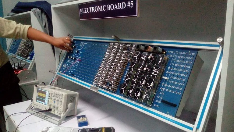
An Electronic training board
Did you ever wonder how the sunlight travels from the sun to your beautiful skin or how the waves in the slam of the waves to our sea borders? Truly, being curious about everything around you makes life great and those things are just types of waves. These waves are all around us even though sometimes we don’t give so much attention to them because we are busy with to dos in life. These waves have specific characteristics of their form, but they also have characteristics in common with more abstract waves like the sound waves and the electromagnetic waves and when projected to a measuring device, their waveforms are displayed to understand more about the behavior of these waves. Some waves are visible to us just like the waves in the ocean but still, some of these waves are not but we can feel them like the seismic waves. Seismic waves are waves of energy that travel through the Earth's layers and are a result of earthquakes and other seismic activities. These waves are measured by an instrument called seismograph and later project their waveforms. The tremors sometimes are minuscule that is difficult to measure in our seismograph. We need some form of amplification so that we can have a better registry for the signal.
In 1904, the vacuum-tube diode was introduced by J. A. Fleming. In 1906, Lee De Forest added a third element, called the control grid, to the vacuum diode. In the following years, radio and television provided great stimulation to the tube industry. On December 23, 1947, Dr. S. Shockley demonstrated the amplifying action of the first transistor at the Bell Telephone Laboratories. In the years to follow, the industry became one of primary importance. The three-terminal solid-state device was smaller and lightweight. It had no heater requirement or heater loss. It was also more efficient since less power was absorbed by the device itself. All amplifiers have at least three terminals, with one controlling the flow or potential between the other two. The transistor was invented in 1947 by W. Shockley, J. Barden, and W. Brattain.
A bipolar junction transistor is type of transistor that is commonly used for amplification or it could be used in switching purposes for it is a type of a device that is a current controlled. It has three terminal sides; the Emitter is the one who emits or supplies any charge carriers, in this part it is heavily doped that is intended for the injection of large charges going to the base section. It is the negative lead part of the transistor. Base is located in the middle layer section in which it is the one responsible for the activation of the transistor. Lastly, the positive lead in the transistor which is the Collector. The collector terminal is responsible in collecting and drawing out the supplied charges.
In bipolar junction transistor, there are two classifications which is the NPN transistor wherein a single p-type layer is in between and is sandwiched by two n-type layers and the other type is the PNP which is the complete opposite of the NPN transistor, a single n-type layer is in between with two p-type layers. The current entering the emitter, base, and collector has a positive sign convention, while the current leaving the transistor has a negative sign convention. Based on the doping forms of the three major terminals, BJTs are graded as NPN or PNP. As compared to the other layers, the emitter area is heavily doped. Charge carrier concentrations are the same in the collector and base layers. The base-emitter junction is forward biased, and the base-collector junction is reverse biased, among these junctions. The p-doped side is forward biased, which means it has more potential than the n-doped side.
An NPN transistor is made up of two semiconductor junctions with a thin p-doped anode region and a thin n-doped cathode region, while a PNP transistor is made up of two semiconductor junctions with a thin n-doped cathode region. The diffusion of charge carriers between the two regions with different charge concentrations induces charge flow in a bipolar junction transistor. This type of transistor's primary use or purpose is to raise current. As a result, they can be used as switches or amplifiers. They're used in a variety of electronic products, including cellphones, televisions, radio transmitters, and industrial control systems.
There are three modes of operations: Cut-off, Saturation, and Active mode. We should know that a biasing voltage is needed to activate the transistor. In Cut-off Mode, the emitter-to-base and collector-to-base junction is in reversed bias condition. In reverse bias condition, there is a restriction of current flow, which means the transistor acts as an open switch. The cut-off area is where the transistor is absolutely switched off and the collector current is zero.
Experiment board.
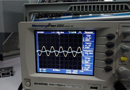
SIgnals shown in the oscilloscope
In saturation mode, the emitter-to-base and collector-to-base junction is at a forward bias state. It allows a current flow through the device. The transistor acts as a closed switch or in “ON” switch. A large charge flows to the base terminal, which it is used to activate the transistor. The transistor is deemed to be operating in "full", but there is no voltage output. When the transistor is completely turned on and operating as a switch, the collector current equals the saturation current. The Active mode focused on current amplification rather than doing active switching. It operates is when either emitter-to-base or collector-to-base junction is in forward bias or reverse bias condition. Typically, it is used in current amplification. The active area is where the transistors are used as amplifiers.
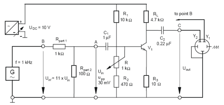
There are three common amplifier set up for BJTs: common bas, common emitter, and common collector. The common base amplifier has voltage gain, but no current gain. In contrast, the common collector does have current gain but no voltage gain. On the other hand, common emitter are most sought because it has has both current and voltage gain. Hence the statics characteristics are different across the set up, we can observe different responses to the input signal from each configuration.
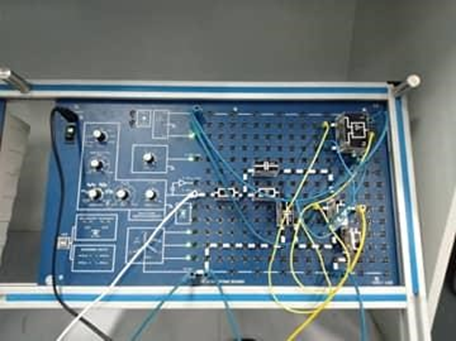
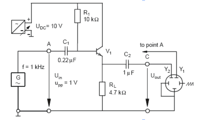
A Common Base Amplifier used in the experiment
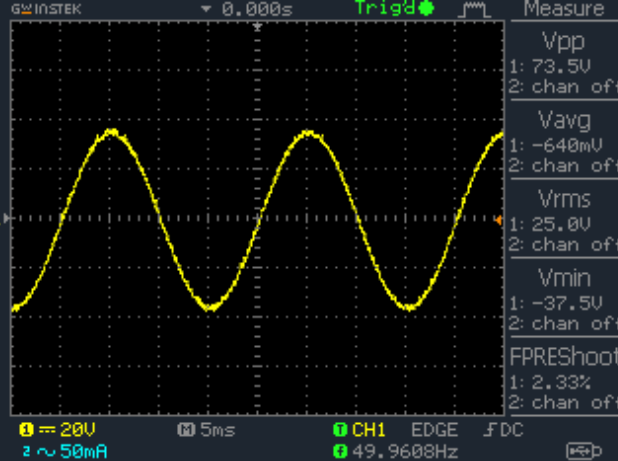
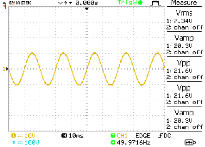
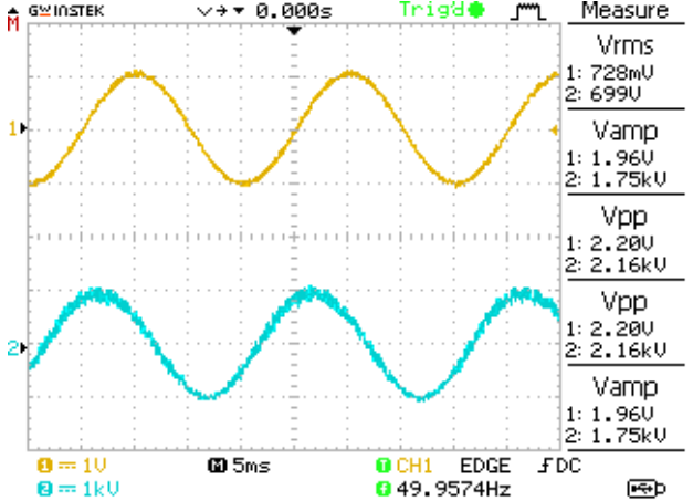
When the base terminal is grounded, we have a common base set up. The base terminal serves as a reference point for the input and output signal. The input signal is applied in the base and emitter terminals, while the output is measured across collector and base terminals. Hence the input current flows into the emitter, it correspond to the sum of the base and collector currents. The collector current output is less than the emitter current input, It results to a current gain of "1" (unity), or less. The common base configuration "attenuates" the input signal.
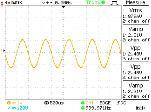
Input signal for the experiment (taken from an oscilloscope)
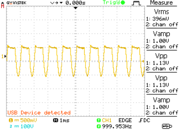
Output signal for the experiment (taken from an oscilloscope)
If we observed the output voltage, we see a attenuated signal. It means that the signal losses some of its amplitude. It adhere to the theoretical response described earlier. The resulting signal is less than to the input signal. It proves that the common base configuration "attenuates" the input signal, which has a gain equal to 1 or less.
A Common Emitter circuit used in the experiment.
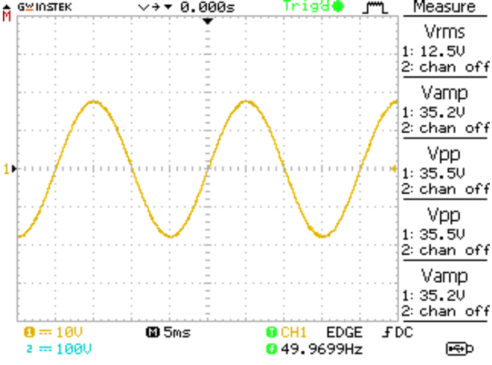
When input signal is applied between the base and the emitter, we have a common emitter. We have a grounded emitter terminal, and we measure the output across the collector and the emitter. It is the most common configuration for transistor-based amplifiers because it gives us current and voltage gain. Among the three bipolar transistor configurations, the common emitter amplifier produces the highest current and power gain. It is due to a low input impedance across forward-biased emitter-to-base junction. In contrast, it has a high output impedance due to the connection to a reverse-biased collector-base junction.
Input signal for the common emitter amplifier
Output signal for the common emitter amplifier
A Common Collector circuit used in the experiment.
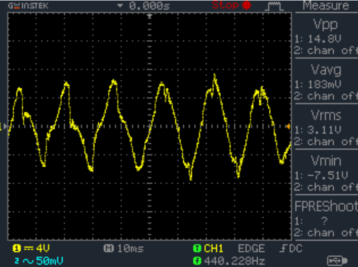
When we grounded the collector terminal, we set a common collector amplifier. Among the configurations, It is not widely adapted due to its restrictive response and characteristics. In common collector, we feed the input signal to the base. We draw the output from the emitter load. It is widely known as a voltage follower or emitter follower circuit.
Input signal for common collector.
Output signal for common collector.
If we focused on the output signal, we can see that the signal is clip off. It is due to very high impedance. We can correct that by properly setting our bias voltage. The common collector is typically used for impedance matching; hence it has very high input impedance, and the relatively low output impedance.
Input and output signal for common collector
In conclusion, a bipolar junction transistor can be used either in switching or for amplification purposes. It is commonly used in various electronics found commonly on our homes jut like the television, mobile phones, computers, radio transmitters, and audio amplifiers. It has also gives a lot of advantages like for example, bipolar junction transistor gives us a high driving capabilities, high frequency operations, or as digital switch.
References
- Boylestad and Nachelsky, Electronic Devices and Circuit Theory
- Floyd, Electronics Fundamentals. Circuits, Devices, and Applications
- Schultz, Grob’s Basic Electronics
Note:
All images are from the author except with separate citation.
https://twitter.com/juecoree/status/1373299557853921285
Thanks for your contribution to the STEMsocial community. Feel free to join us on discord to get to know the rest of us!
Please consider supporting our funding proposal, approving our witness (@stem.witness) or delegating to the @stemsocial account (for some ROI).
Please consider using the STEMsocial app app and including @stemsocial as a beneficiary to get a stronger support.